The field of machine learning has experienced explosive growth over the past decade, driven not only by algorithmic advances but also by significant improvements in specialized computing hardware. This symbiotic relationship between algorithms and hardware has enabled the development of increasingly sophisticated AI models that were previously computationally infeasible, and 2026 has been the year that relationship produced its most dramatic hardware generation yet, with NVIDIA, Google, AMD, and AWS all shipping purpose-built accelerators aimed squarely at trillion-parameter-scale training and inference.
The GPU Revolution
Graphics Processing Units (GPUs), initially designed for rendering video games, found an unexpected application in machine learning. Their parallel architecture, capable of handling thousands of simple calculations simultaneously, proved ideal for the matrix operations that form the backbone of neural networks.
NVIDIA’s CUDA platform provided the foundational software layer that allowed researchers to harness GPU power for general-purpose computing, first released in 2007. This democratized access to parallel computation, enabling the training of larger models and processing of bigger datasets than ever before. Every major deep learning framework, from PyTorch to TensorFlow to JAX, still compiles down to CUDA kernels (or a ROCm/AMD equivalent) at the bottom of the stack, which is why GPU driver and toolkit versioning remains one of the most common sources of environment-setup pain in ML engineering to this day.
However, GPUs were, and still are, general-purpose processors adapted for ML workloads. That “adapted for” gap is exactly what the last decade of specialized silicon has been trying to close.
The Rise of TPUs
Google’s Tensor Processing Units (TPUs) represented the first major foray into hardware specifically designed for machine learning workloads. Unlike GPUs optimized for graphics rendering, TPUs were architected from the ground up for tensor operations, the fundamental computation in neural networks: large matrix multiplications executed at reduced numerical precision.
TPUs introduced several innovations that are now standard across the specialized-AI-silicon industry:
- Matrix multiplication units (systolic arrays): dedicated hardware for the core operation in neural networks, rather than general-purpose ALUs repurposed for it
- High-bandwidth memory (HBM): stacked memory placed physically next to the compute die to minimize the data-movement bottleneck that dominates real-world accelerator performance
- Quantization support: hardware-level support for lower-precision formats (FP8, FP4) that trade a small amount of numerical accuracy for large throughput gains
- Custom instruction sets: tailored to the specific operations that show up in transformer training and inference, rather than a general instruction set
Google’s seventh-generation TPU, codenamed Ironwood (TPU v7), reached general availability on April 22, 2026. Each Ironwood chip delivers 4,614 FP8 TFLOPS with 192 GB of HBM at roughly 7.37 TB/s of bandwidth, and a full pod scales to 9,216 chips for a combined 42.5 exaflops — Google describes it as a more than 4x per-chip improvement over the prior TPU v6e (“Trillium”) generation, and the company’s own materials explicitly position it as its first TPU generation designed primarily for inference rather than training (Ironwood: The first Google TPU for the age of inference, Google Blog; Ironwood TPUs and new Axion-based VMs, Google Cloud Blog).
The 2026 Accelerator Landscape
Following Google’s lead, every major compute vendor now ships (or is about to ship) hardware purpose-built for AI rather than adapted from an existing product line.
NVIDIA’s Blackwell Platform
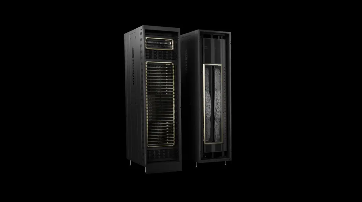
NVIDIA’s current-generation Blackwell architecture centers on the B200 GPU, a dual-die design with 208 billion transistors, 192 GB of HBM3e, and 8 TB/s of memory bandwidth, delivering up to 9,000 TFLOPS at FP4 precision — NVIDIA states this is roughly 4x the inference throughput of the previous Hopper-generation H100 (NVIDIA Blackwell Platform Arrives, NVIDIA Newsroom). The rack-scale GB200 NVL72 system pairs 36 Grace CPUs with 72 Blackwell GPUs behind a single 130 TB/s NVLink domain that NVIDIA markets as functioning like one enormous GPU, claiming up to 30x faster real-time inference on trillion-parameter models versus the Hopper generation it replaces (GB200 NVL72, NVIDIA).
AMD’s Instinct MI350 and MI400 Series
AMD’s current Instinct MI350X/MI355X GPUs, built on CDNA4 and TSMC’s 3nm process with 185 billion transistors across 256 compute units, ship with 288 GB of HBM3e at 8 TB/s. AMD has already confirmed the follow-on MI400 series, built on the new CDNA5 architecture, for launch in the second half of 2026, with 432 GB of HBM4 memory, 19.6 TB/s of bandwidth, and up to 40 petaflops of FP4 compute per chip (AMD Instinct MI350 Series and Beyond, AMD).
AWS Trainium3: Custom Silicon at Hyperscaler Scale
Amazon’s fourth generation of custom AI silicon, Trainium3, became generally available in December 2025. Fabricated on TSMC’s 3nm N3P process, each chip delivers 2.52 petaflops of MXFP8 compute with 144 GB of HBM3e, and Amazon’s own materials state that Trn3 UltraServers (scaling up to 144 chips) deliver up to 4.4x higher performance and 4x better performance-per-watt than the prior Trn2 generation (Trainium3 UltraServers now available, Amazon). The strategic logic is straightforward: training and serving models on AWS’s own silicon instead of purchased NVIDIA GPUs materially lowers Amazon’s own cost per token, which is why every major hyperscaler (Google with TPUs, AWS with Trainium, Microsoft with Maia) now runs a parallel custom-silicon program alongside its NVIDIA GPU fleet.
Wafer-Scale: Cerebras’s Different Bet
Cerebras took a structurally different approach: instead of connecting many separate chips together, the WSE-3 is a single 46,225 mm² piece of silicon (fabricated on TSMC 5nm) containing 4 trillion transistors and 900,000 AI-optimized cores, with 44 GB of on-chip SRAM reachable at roughly 21 petabytes per second of internal bandwidth — Cerebras designs around manufacturing defects with redundant cores and routing rather than trying to avoid them entirely, which is what makes wafer-scale manufacturing viable at all (Cerebras WSE-3 chip specifications, Cerebras).
Accelerator Comparison (2026)
Note that these figures aren’t perfectly apples-to-apples — vendors report peak throughput at different numerical precisions (FP4 vs. FP8), and Cerebras reports a blended “AI compute” figure for its wafer-scale design rather than a chip-level TFLOPS number — but the relative memory capacity, bandwidth, and generational trend are directly comparable:
| Accelerator | Vendor | Memory | Memory Bandwidth | Peak Compute | Best Suited For |
|---|---|---|---|---|---|
| B200 / GB200 NVL72 | NVIDIA | 192 GB HBM3e (per GPU) | 8 TB/s (per GPU) | ~9,000 TFLOPS FP4 | General-purpose training + inference, broadest software ecosystem |
| TPU v7 “Ironwood” | 192 GB HBM (per chip) | 7.37 TB/s (per chip) | 4,614 TFLOPS FP8 (per chip) | Large-scale inference, JAX/TensorFlow workloads on Google Cloud | |
| Instinct MI400 (H2 2026) | AMD | 432 GB HBM4 (per chip) | 19.6 TB/s (per chip) | 40 PFLOPS FP4 (per chip) | Memory-bound large models, ROCm-based training |
| Trainium3 | AWS | 144 GB HBM3e (per chip) | — | 2.52 PFLOPS MXFP8 (per chip) | Cost-optimized training/inference within AWS |
| WSE-3 | Cerebras | 44 GB on-chip SRAM | ~21 PB/s (on-chip) | 125 PFLOPS (blended) | Single-device training of models that would otherwise require large GPU clusters |
The Impact on Model Development
Specialized ML hardware has enabled the development of models with unprecedented scale:
- Larger models: hardware improvements have made it feasible to train models with hundreds of billions to trillions of parameters
- Faster training: what once took months can now be accomplished in days or weeks
- More experiments: researchers can iterate more quickly, testing multiple hypotheses in parallel
- Real-time inference: complex models can now run efficiently enough for real-time, latency-sensitive applications, which is the specific problem Google says Ironwood was built to target
Challenges and Considerations
Despite the advances, several challenges remain, and if anything they’ve gotten more acute as the hardware has scaled up:
- Cost: a single GB200 NVL72 rack or an equivalent TPU pod allocation represents a multi-million-dollar capital commitment, which concentrates frontier-model training in the hands of a small number of well-capitalized labs and hyperscalers
- Energy consumption: large-scale AI training and inference now consumes enough electricity that data center power availability, not chip supply, is increasingly the binding constraint on how much compute hyperscalers can actually deploy
- Accessibility: the complexity of optimizing a given model for a specific hardware backend (CUDA vs. ROCm vs. XLA/TPU vs. Cerebras’s own software stack) can be prohibitive for smaller teams, which is part of why NVIDIA’s broader software ecosystem remains a competitive moat even when a competitor’s chip wins on raw spec sheet numbers
- Software fragmentation: managing different hardware backends across a single organization’s training and inference stack adds real engineering overhead that doesn’t show up on a spec sheet
The Future of ML Hardware
Looking ahead, expect continued specialization rather than consolidation: Google, AMD, and AWS have all already confirmed their next-generation chips are in development, and the frontier labs training the largest models increasingly co-design their model architectures around the specific accelerator they’ll run on, rather than treating hardware as a fixed, interchangeable substrate underneath an architecture-agnostic model.
This symbiotic evolution of hardware and algorithms will continue to push the boundaries of what’s possible in artificial intelligence, enabling new applications and capabilities that would be computationally infeasible on last generation’s silicon.
If you’re speccing an actual workstation rather than following hyperscaler-scale silicon, our sister site TensorRigs covers what’s realistic to actually buy today, from consumer RTX cards up to H100-class hardware, in its Best GPUs for Deep Learning 2026 guide.